Material Gains
The following story originally appeared in the Fall 2018 edition of Baylor Arts & Sciences Magazine. Click here for the complete story.
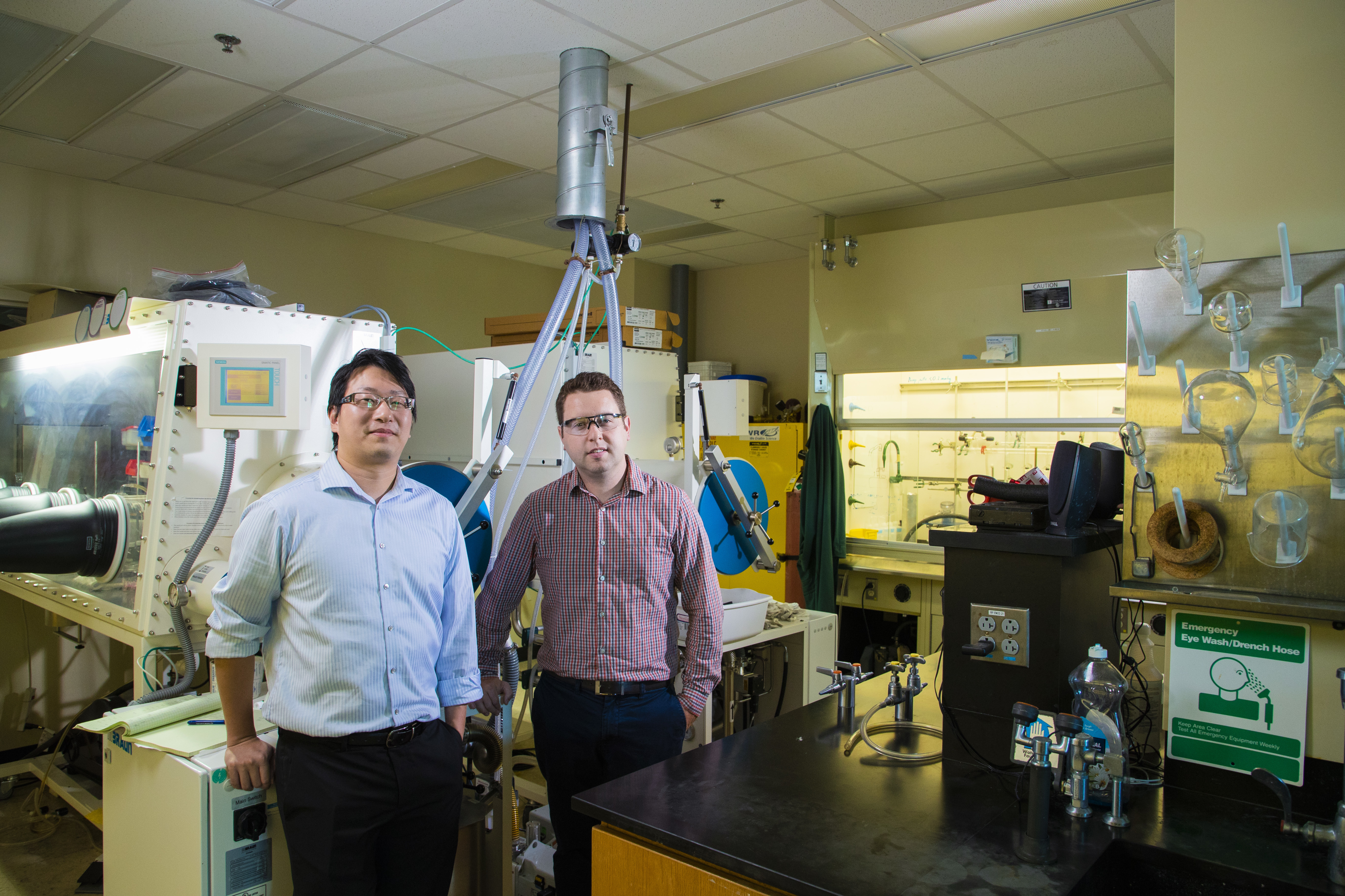
Earlier this year, two junior faculty members in the Baylor College of Arts & Sciences each received the most coveted grant awarded by the National Science Foundation to young researchers –– Caleb Martin, Ph.D., assistant professor of chemistry, and Howard Lee, assistant professor of physics. Not only was the twin win unprecedented at the University, but it also underscored the growing importance of the research in the field of materials science done by the two honorees –– research that promises to make a significant impact on future technology.
“This is the first time that two College of Arts & Sciences faculty members have received this honor in the same year,” said Dr. Kevin Chambliss, associate dean for research and graduate education in the College of Arts & Sciences. “Dr. Martin and Dr. Lee have also received nationally competitive funding from other sponsors. Their accomplishments to date are an exemplary model for other junior faculty to emulate as Baylor moves forward along the trajectory of becoming a preeminent Christian research university with Carnegie ‘R1’ status.”
Chambliss said most junior faculty members in the sciences aspire to receive an NSF CAREER award, which are given to those who show the exceptional promise of an early-career investigator in research, education and public outreach.
The science of stuff
Both Martin and Lee are working on projects that fit neatly under the multidisciplinary umbrella of materials science, which, simply put, is really the science of “stuff.”
Researchers in chemistry, physics and biology are responsible for the discovery of new materials or the improvement of existing materials, be they naturally or synthetically derived. And sometimes, these discoveries are serendipitous. In the earliest stages, research projects like Martin’s or Lee’s don’t necessarily begin with a specific application in mind, either.
“In my research group we’re synthetic chemists, and we are interested in compounds featuring the element boron that have unique properties,” Martin said. “We make the compounds that would potentially be an ‘individual layer’ or ‘component.’ Then, someone who would apply or advance the technology further –– an engineer –– would design and fabricate a device using our new chemical component. Engineers don’t have the expertise to make the compounds or components, but they know how to take what we make and put it together to advance the technology. Ultimately, to make an impact on research problems, it is critical to involve experts in all areas.”
Whether they know it or not, Martin said virtually everyone benefits by advances in materials science, from consumers to corporations, as well as the state.
“The military agencies fund a lot of materials research — Kevlar, for instance, would be a material,” Martin said, referring to the well-known, bullet-resistant component in body armor, combat helmets, ballistic face masks and ballistic vests. “With materials, what we’re considering is anything that’s a solid that can perform some function.”
Another popular product of materials science is Teflon, accidently discovered in 1938 by a researcher working for DuPont. Teflon is the key compound in the coating that slicks non-stick frying pans and countless other surfaces. Teflon has applications on land, sea and in the air –– from coatings for the bottom of large ships, making them resistant to barnacle adhesion (which causes resistance and ultimately requires more fuel for transport), to protective coatings on spacecraft.
Light and power
Both Martin’s and Lee’s research groups focus on components that will eventually benefit a variety of electronic or optical devices and systems.
Martin’s five-year, $650,000 CAREER grant, funded through the NSF’s Chemical Synthesis Program, will support his group’s research into organoboron chemistry.
“We’re trying to take advantage of the unusual conductive properties that boron presents, particularly the ability to transport electrons much more easily than existing state-of-the-art materials,” Martin said.
This special capability makes these boron compounds useful for organic light-emitting diodes (OLEDs) that are used to create digital displays in common, everyday devices including TVs, computer screens and mobile phones.
“With OLEDs, there are always improvements in the technology that can be made by getting more efficient components, which decrease the amount of electricity required and the size,” Martin said. “With this in mind, thinner and smaller devices can be made based on the efficiency of each individual component.”
Martin’s research also stands to impact the efficiency of solar panels. A phenomenon known as the photovoltaic effect is the reason why solar panels on roofs and buildings can convert absorbed sunlight into electricity to power homes and businesses. First observed in 1839, the photovoltaic effect is both a physical and chemical property — essentially the generation of voltage and electric current in a given material when that material is exposed to light.
“Organic solar cells, such as ones that could be made incorporating boron, are not as common, but they do offer advantages over inorganic ones,” Martin said. “The ones you see on roofs are inorganic. These contain toxic heavy metals and lack flexibility. Organic devices, by contrast, do not contain these metals and offer the advantage of flexibility.”
Here in the United States, as population growth and other factors drive the cost of electricity higher and higher, many states are beginning to lean more heavily on solar power. Beginning in 2020, California will become the first state to require all newly built homes to have solar power, while other states including New Jersey and Massachusetts are also looking at legislation that would require all new buildings be solar-ready.
Equally as timely, Lee’s research involves a super-thin film –– a metasurface –– that can serve as a “perfect absorber” of light, according to Lee. His research group received a five-year, $500,000 CAREER Award to develop these metasurfaces, whose soon-to-be patented nanostructure makes them electrically tunable — that is, they are capable of changing the properties of light.
(For reference, prefixes “meta” and nano” allow scientists and engineers to discuss materials that are so unbelievably small, they exist on their own scale. A nanometer is one billionth of a meter. And Lee’s metasurfaces are 1,000 times thinner than the width of a human hair).
“The key thing here is that we’re making these metasurfaces really thin,” Lee said. “And this surface can absorb 100 percent of the light that falls on it.”
The virtual weightlessness and absorptive capacity of Lee’s metasurfaces alone could significantly improve the efficiency of photovoltaic solar cells and other light-absorbing devices.
In other variations of this ultra-thin film, by changing the electrical voltage applied to the film these metasurfaces may filter out specific colors on the electromagnetic spectrum, or actually direct or steer beams of light. Lee said this ability to manipulate the electro-optical properties of this film by controlling the voltage is what makes this project so unique.
“If you can control the light really well using this nanostructure, you can design all the optical properties such as transmission and absorption of light,” Lee said. “You can filter the light so that only one color is transmitted or absorbed.”
Though research into this kind of ultra-slim optical film is still a few years away from any material application, Lee said several companies have already expressed an interest, including Google, Samsung and Sony.
“We really want to demonstrate the electrical tunability of the film, so we are trying to develop prototypes to show functionality for the perfect absorber, the color filter and the beam-steering metasurfaces,” Lee said. “At the moment, no one is actually demonstrating all of these properties efficiently.”